Caveats: |
I wrote this article 6-1/2 years ago. Even though some of the techniques of memory size have changed since then, the basic concepts are still the same. Forgive me if you see some outdated terms, or references to outdated CPU's and memory sizes. If you see some instances of outdated material, instead of sending me flames, please send a kind note of correction. |
The concepts of memory
sizing wouldn't be complete without an explanation of how
RAM works. Think of memory as a square, two-dimensional
array; there are as many columns as rows. Each element in
the array represents a bit (not byte) of memory. To
address an individual bit in the array, we provide the
RAM chip with a row address and a column address. To
minimize the number of pins on the chip, RAM chips have
only one set of address pins, and uses them for both row
and column addresses (see
figure 1). The memory controller must provide signals
telling the RAM chip when the row address is valid via
the Row Address Strobe (RAS), and when the column address
is valid via the Column Address Strobe (CAS). The concept
of using a single set of address lines for both row and
column addressing is called multiplexing (MUX). As a
result of multiplexing the address lines, RAM chip sizes
are always a square power of 2 (or even multiple of 2).
Chips with 8 address lines hold 64k bits of information
((28)2 = 65536); 9 address lines
yield 256k chips ((29)2 = 262144),
10 address lines yield 1M chips, and so on. Now, armed with this information, we can discuss the relationship between the CPU address bus and the memory address bus. The CPU has 24 address pins if it is a '286, and 32 address pins if it's the '386, '486, or Pentium; 36 address pins if it's a Pentium Pro. The RAM chips obviously have far fewer address pins than the CPU; so to convert the CPU address to RAM RAS & CAS addresses, the CPU address bus enters a memory controller. The memory controller converts the CPU address signals to RAS addresses, CAS addresses, and BANK addresses (more on BANK addressing later). Let's suppose our computer was a '286 design supporting only 4 banks of memory. (Even though the 80286 is obsolete, describing it's memory configuration is perfect for this example.) This memory can consist of any combination of 64k, 256k, 1M, and 4M chips, but each bank must be populated with a consistent size of RAM chips. To support 4M memory chips, our memory controller must provide signals to 11 RAS addresses, plus 11 CAS addresses. This takes 22 of our 24 address lines available from the CPU. The remaining two address lines from the CPU are interpreted by the memory controller to select which BANK of memory to access. Figure 2 shows a hypothetical relationship between the CPU address bus and the memory address bus. According to this diagram, anytime the CPU asserts A00..A10, the RAM chip receives a column address. Likewise, anytime the CPU asserts A13..A23, the RAM chip receives a row address. CPU address lines A11 and A12 are used to select between RAM banks. Since our hypothetical computer supports only four banks of memory, when <A12,A11>=00, the memory controller selects BANK0; when <A12,A11>=01, the memory controller selects BANK1; <A12,A11>=10 the memory controller selects BANK2; and <A12,A11>=11, the memory controller selects BANK3. With this information, we can write to any row of any bank of RAM chips in the computer. In this manner, we can detect how many banks of RAM are installed in the computer, and determine the size of each RAM bank. All that we need to complete our RAM sizing discussion is some theory and algorithms to apply our knowledge. In our hypothetical computer, the memory controller multiplexes the addresses according to the size of RAM chips. Figure 2 showed the CPU address bus/memory address bus relationship for 4M chips. When the chip size is smaller than 4M, the relationship between the CPU address bus and RAM address bus changes. In our computer, chip size in each RAM bank is programmable; therefore we need to determine the size of the chip in the socket and subsequently re-program the memory controller before we can have full access to all the memory in the computer. To size memory, we start by assuming each RAM bank has the maximum size RAM chips which are supported by the memory controller. In our hypothetical computer, the memory controller supports up to 4M chips. Therefore, we program the memory controller for four banks of 4 MB chips. By programming the memory controller for this configuration, we can detect when a smaller memory chip is installed in the socket. But before we check the size of the chip, we need to detect if any RAM is in the socket. RAM detection is achieved by writing to the RAM bank, completely reloading the prefetch queue, and checking the value we wrote. If we get back the value we wrote, we have sufficiently determined that RAM is available for that bank of memory. And then we can check the size of the chip. |
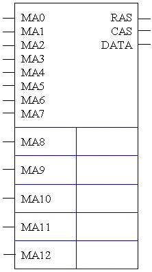
Figure 1 - 64k, 256k, 1M, 4M,
64M, 256M Figure 2 - CPU Address Bus Conversion |
To determine the actual size of RAM, we need to detect how many address lines are connected to the RAM chip. Consider the 11 address lines on our 4 MB RAM chip socket. If our RAM is a 4M chip, then all 11 address lines are connected (MA0 - MA10). If the RAM chip is a 1M chip, only 10 address lines are connected (MA0 - MA9); 256k has 9 lines connected (MA0 - MA8); and 64k has 8 lines connected (MA0 - MA7). To determine whether a 4M chip is installed, we need to determine if MA10 is connected. We write to MA10, then read back at RAM address 0 (MA0-MA10 not asserted). If a 4M chip is in the socket, then the data we wrote at MA10, will appear at MA10, and not at RAM address 0. But if the RAM chip isn't a 4M chip, then MA10 isn't connected; therefore the data we wrote at MA10 would have been written to address 0. Our algorithm repeats itself by using MA9 for 1M chips and MA8 for 256k chips. If MA8 - MA10 all fail, then it is safe to assume the bank is populated with 64k chips, as we already determined the presence of RAM in the socket.
To determine how many banks of memory are in the computer, we test the existence of RAM for each bank. This is done by writing to the CPU address lines that control RAM bank selection. For our computer, these are address lines A11 and A12.
By repeating this RAM sizing algorithm for each bank of memory, we can determine how much RAM is installed in the computer. Figure 3 summarizes the relationship between Multiplexed Addresses (MA) on the RAM address bus, and CPU addresses on the CPU address bus. The CPU addresses in this figure are calculated from the table of MA addresses. If we need to assert <A23>, <A11>, and <A12>, then we calculate the CPU address as 223 + 211 + 212 = 801800h.
To summarize: knowing the relationship between CPU addresses, RAM row and column addresses, and bank selection addresses is essential to determining RAM size and quantity. RAM Bank selection is done by writing to the CPU address lines that are interpreted by the memory controller as controls for bank selection. RAM sizing is done by writing to the highest RAM ROW address for a given chip size and reading the RAM at 0. If the data appears at 0, you know the RAM ROW address line on the chip isn't connected. Continue this process until all RAM sizes are determined for each bank. At the completion of this process, we re-program the memory controller for the proper RAM configuration in the system.
Sizing RAM under program control is accomplished differently than it was during the power-on sequence. During the power-on sequence, the BIOS is guaranteed absolute control of the system, and its resources. During this sequence, BIOS can guarantee that cache is disabled so that it won't interfere with the results. Under program control, we can't write a RAM sizing algorithm that makes any assumptions about the state of the hardware or the cache. If we re-program the memory controller, our program would most certainly fail, as CPU address translation changes with the RAM address translation. In determining the amount of RAM under program control, we must use a different approach, an approach that doesn't rely on knowledge of the hardware. This means we can't re-program the hardware, the memory controller, or the cache controller. Since we can't re-program the memory controller (or make any assumptions about the existence, state, or programmability of a cache controller), we must write an algorithm that can detect the presence of memory without the intrusion of cache RAM. Therefore, the algorithm must be able to invalidate the cache RAM contents while checking for the existence of memory.